|
|
Analog ICs for 3V Systems Single 3V operation is available for many op amps, comparators, and microprocessor supervisors, and for some RS-232 interface ICs. For A/D and D/A converters, analog switches, and multiplexers-which often require minimum supply voltages of 5V or ±5V-the choice is more limited. You can, however, easily provide the required voltages with a local switching regulator or charge-pump converter. Though 3V designs are beginning to appear across the board, the switch to low voltage is most notable in systems for which size, weight, and power consumption are especially critical-palmtop computers and wireless phones, for example. And, with the increasing demand for small size and longer battery life, it is likely that blood analyzers, barcode scanners, data loggers, and other portable equipment will also follow suit. The switch from 5V to 3V also benefits line-powered systems, because the lower power dissipation associated with 3V operation allows smaller power supplies, heatsinks, and fans. The change from 5V to 3V also means that higher-density, higher-speed logic can operate at the same level of power dissipation. The following discussion covers 3V analog ICs, the power savings inherent in their operation, and the problems associated with low-voltage operation. It also presents methods for generating 5V from 3V, and methods for generating 3V from inputs that range above and below 3V (such as the terminal voltage of a 3-cell alkaline battery). Power Savings from 3V Operation Many new op amps, microprocessor supervisors, and interface ICs (along with a handful of A/D and D/A converters, voltage references, and switches) are now specified for 3V operation. The following sections discuss these product types in detail. Interface
Transceivers RS-232 appeared in the days of mainframe and mini computers, at a time when ±12V power supplies were common in such systems. Not surprisingly, the first RS-232 transceivers required ±12V for operation. Voltage drops internal to the IC reduced the output swing to about ±9V, so the required minimum was set still lower, at ±5V. Now (32 years later), the RS-232 standard is still around, with the official name of EIA/TIA-232-E (or 232E for the sake of brevity). The advent of portable and low-voltage equipment has spawned a new serial-interface specification that can replace the 232E standard. Called EIA/TIA-562 (562 for brevity), this new standard became effective in 1991. The 562 and 232E standards are electrically compatible, so the new 562 designs will mate with existing 232E equipment and vice versa. For a comparison of certain 232E and 562 specifications, see Table 1. Note that the driver output swings differ (±5V vs. ±3.7V), but the receiver input thresholds are the same (±3V). The 562 devices' ±3.7V minimum output swings allow them to communicate with 232 receivers, which have input thresholds of ±3V. The noise margin, however, is only 0.7V. By comparison, the 232 drivers' ±5V minimum swings guarantee a noise margin of 2V. Table 1. Comparison of 232E and 562 Interface Standards
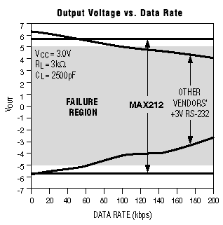
The 562 standard cuts power consumption by specifying a minimum output swing of ±3.7V (vs. ±5V for 232E). The resulting power consumption for 562 drivers is only 55% of that required for 232E drivers. Note that line drivers (not the receivers) consume most of the power. Therefore, a palmtop computer containing 562 interface ICs provides power savings whether it connects to a 562 receiver or a 232E receiver. Maxim has four 3V interface ICs that comply with the 562 standard. Each includes a charge-pump converter for generating the required output-voltage levels. The charge pump doubles VCC to create the positive level, then inverts that voltage to create the negative level. For a given IC, the required external charge-pump capacitors (a set of four) have values of either 0.1µF or 1.0µF, with the larger value supporting a larger number of drivers and receivers. The MAX563, for example, has two drivers and two receivers, and operates with four 0.1µF capacitors. Its 116k bits per second (116kbps) data rate makes it compatible with LapLink™ software. It also provides a 10µA shutdown mode in which the receivers remain active. This feature-active receivers during shutdown-extends battery life in portable applications. It enables the computer to monitor external devices such as the ring indicator of a modem, via the serial interface, with minimal power consumption. In remote data gathering, for example, the computer may spend much of its time waiting for a ring signal or other external stimulus. If the computer and the interface IC have no access to AC power, both can remain shut down until "awakened" by the external signal. Maxim also offers RS-232 transceivers that operate from 3V. These chips include special high-efficiency DC-DC converters for generating the higher output swings specified by EIA/TIA-232E. High efficiency is attractive because RS-232 loads can consume several hundred milliwatts at high data rates. Some manufacturers include charge-pump voltage triplers in their 3V interface ICs, but these ICs dissipate considerable power, and are unable to sustain the ±5V minimum outputs at higher data rates. Though effective in compensating for voltage drops in themselves and in their driver-output stages, voltage triplers are less efficient than the doublers used in 5V ICs. Miniature on-chip switching regulators are the most efficient at generating RS-232 voltages. That's why the new 3V RS-232E transceivers from Maxim contain efficient switching regulators rather than voltage triplers. Switchers draw 50% less current than do charge-pump triplers. They also provide outputs suitable for powering mice and supporting high data rates (such as 116kbps for LapLink™). Other vendors' charge-pump-tripler ICs can't necessarily meet the drive requirements of a mouse (10mA at 5V and 5mA at -5V). Nor can they necessarily provide the minimum output levels (±5V) required by 232E at high data rates (Figure 1).
Figure 1. Maxim's 3V RS-232 transceivers, which derive their output-signal levels from a low-cost switching regulator, maintain valid levels at high data rates. Those with charge-pump triplers (from other vendors) do not. Because many receivers have TTL voltage thresholds, it may be acceptable for an RS-232 output to fall below 5V while transmitting to another RS-232 device. Sub-5V RS-232 levels for the mouse, however, may cause it to fail. The mouse steals power from the RS-232 line to supply an internal microcontroller, whose minimum supply voltage in most cases is slightly below 5V. The components used in the switcher and charge-pump-tripler approaches are equivalent in cost and size.
The 3V MAX212, an RS-232 transceiver with three drivers and five receivers in a 24-pin package, produces ±6.5V with a single-inductor, double-duty switching regulator. The MAX218 employs a different approach. This two-driver/two-receiver IC produces a positive output level with a boost switching regulator, and a negative output level with an inverting charge pump (Figure 2). 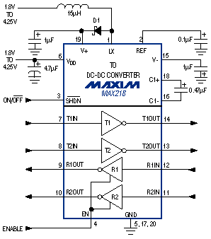
Figure 2. This low-voltage interface IC includes a high-efficiency DC-DC converter, which generates the voltages required for RS-232 communications. The MAX218 operates from 3V VCC or a 2-cell battery (minimum voltage 1.8V), with a guaranteed data rate of 120kbps. Its two receivers remain active during the 1µA shutdown mode, enabling the chip to monitor external devices while consuming small amounts of power. Packages include 20-pin DIPs, SOs, and SSOPs. A/D Converters Low power consumption is a critical attribute for A/D converters operating in portable equipment. These applications often require high speed as well, but high speed and low power tend to be mutually exclusive. Accordingly, manufacturers have produced a new type of A/D converter-one that draws moderate supply currents while acquiring data, but very low currents while in shutdown. The result is a power savings for converters that operate intermittently. The MAX152, for example, is a half-flash A/D converter whose 1.8µs conversion time produces a throughput of 400k samples per second (400ksps). Operating on 3V or ±3V, it accepts unipolar or bipolar inputs. The 1.5mA operating current drops to 1µA in shutdown mode. Because the MAX152 returns from shutdown to full operation with the first acquired sample in less than 900ns, it can offer a large power savings for applications in which the sampling is intermittent (Figure 3). 
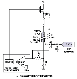
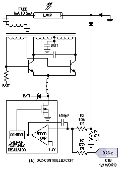
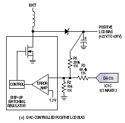
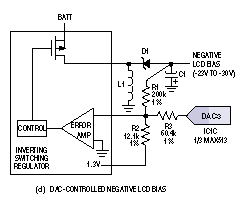
Figure 3. By entering a 1µA power-down mode between conversions, the MAX152 8-bit A/D converter offers a dramatic reduction in supply current. One such application is the measurement of received signal strength in cellular telephones (RSSI: received signal-strength indicator). The MAX152 digitizes the signal at 2ksps while drawing a mere 15µA from the 3V supply. Total unadjusted error (the sum of offset, integral nonlinearity, and gain errors) less than 1LSB is guaranteed, and SINAD (signal-to-noise and distortion) less than 45dB is guaranteed. The MAX152's 20-pin SSOP or DIP is ideal for space-sensitive applications. D/A Converters New ICs also allow 3V digital systems to generate analog outputs. Intended for portable applications, these ICs require very little power and board area. The low-cost MAX513, for instance, is an 8-bit, voltage-output, triple D/A converter. Its low operating current (1mA) and low shutdown current (1µA) are ideal in portable applications, and its serial-data control allows it to fit into 14-pin DIP and SO packages. The MAX513 operates from single or dual supplies, and its outputs swing to within 500mV of the rails. It has two buffered outputs plus a third, unbuffered output that allows the user to achieve higher precision. The MAX513 is attractive for low-cost applications such as trimming offset voltages, setting the bias point for adjustable current (or voltage) sources, and setting the regulation point in other circuits (Figure 4).
Figure 4. The MAX513 triple, 8-bit D/A converter single-handedly controls three notebook-computer functions: battery charger (a), bias for cold-cathode flourescent tube (CCFT) (b), and positive (c) or negative (d) bias for the liquid-crystal display. Op
Amps Three-volt operation not only reduces the signal range, it puts an additional squeeze on SNR by raising the noise floor. Low-voltage amplifiers typically draw low supply current, which leads to higher levels of amplifier noise. In addition, the feedback resistors have higher values (to limit system supply currents), which also adds noise to the system. To further complicate matters, high-impedance nodes are more likely to pick up noise from high-speed digital signals via capacitive coupling. You should, therefore, keep high-impedance traces short and physically distant from high-speed digital traces. Noteworthy features for the new 3V op amps include ultra-low supply current (1µA), low offset voltage (60µV), and high speed (10MHz). Devices in the MAX492 series, for example, combine a 600kHz gain-bandwidth product and 200µV offset voltage with a low 130µA supply current. Input ranges are rail-to-rail, and outputs swing within 150mV of either rail. These characteristics make the MAX492 op amps useful as instrumentation amplifiers in low-voltage, battery-powered systems (Figure 5). 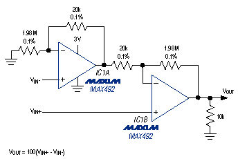 Figure 5. A wide output-voltage swing and precision (200µV offset) make this dual op amp a good choice for low-power instrumentation amplifiers. The instrumentation amplifier of Figure 5 illustrates the larger
dynamic range available with a wider output-voltage swing. Gain is
100(VIN+ - VIN-) and the rails are 3V and 0V, so the maximum
differential input voltage (28.5mV) produces a full-scale output of 2.85V.
(The 10k Among the newest 3V op amps are the first available monolithic, bidirectional, high-side current-sense amplifiers-the MAX471 and MAX472. These devices minimize grounding problems by eliminating current-sense resistors in the low-side ground returns of portable PCs, handiterminals, and other battery-powered systems (Figure 6). Both come in 8-pin packages. 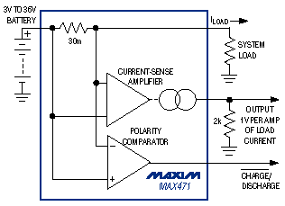 Figure 6. The MAX471 is the first available monolithic, bidirectional current-sense amplifier. With the addition of a gain-setting resistor, it forms a complete current-to-voltage converter. The MAX471's 30m Thus, the MAX471 can monitor charge the way a gas gauge monitors gas, yielding a so-called battery gas gauge: connecting an A/D converter to the MAX471 output allows a microcontroller to track the battery's status by monitoring incoming and outgoing charge. The MAX472, similar to the MAX471, adds design flexibility with a user-specified external current-sense resistor. Both devices operate on 3V to 26V, draw less than 100µA, and conserve power with a 12µA shutdown mode. For portable applications that must conserve every microamp, some 3V micropower op amps offer remarkably low supply currents. At 1.2µA maximum, the MAX406/MAX407/MAX409 and MAX417-MAX419 devices offer the lowest power consumption available anywhere. Outputs swing from the negative rail to within 1.1V of the positive rail, and input ranges include the negative rail. The MAX406 (single), MAX407 (double), and MAX418 (quad) op amps are unity-gain stable with 8kHz gain-bandwidth products. The MAX409 (single), MAX417 (dual), and MAX419 (quad) devices are stable for gains 10V/V and higher, and have 150kHz gain-bandwidth products. All of these low-power devices operate between 2.5V and 10V or between ±1.25V and ±5V. Low-voltage data-acquisition systems often require a negative reference voltage. Placing a positive reference in the feedback path of a MAX406 op amp, for example, produces a -2.50V reference (Figure 7). The op amp and positive reference are low-power devices, so the total current drain is only 11µA. This arrangement eliminates the feedback resistors and associated errors found in a standard inverting configuration. 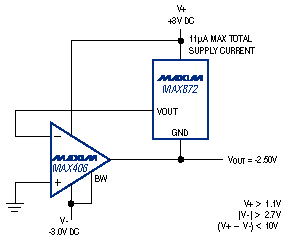 Figure 7. This negative reference, obtained by placing a positive reference in the feedback path of an op amp, draws only 11µA. Also, driving the load with an op amp eliminates any degradation of the reference voltage by load-regulation errors. The amplifier's input common-mode range determines the minimum required positive supply voltage, and the reference dropout voltage determines the minimum negative supply. These supply voltages need not be carefully regulated; the positive one can fall as low as 1.1V, and the negative one can rise as high as -2.7V. Comparators The MAX941's combination of low voltage and high speed is without parallel-it excels, for example, as an overcurrent monitor in 3V systems (Figure 8). The circuit of Figure 8 monitors load current through the low-side current-sense resistor R1, and compares it with a 100mV reference developed by IC1 and resistors R2 and R3. When the R1 voltage exceeds 100mV, the comparator output goes high and turns off the Q1 power MOSFET. The comparator remains latched in this state because it drives its own latch input (pin 5). A positive pulse at the base of Q2 unlatches the circuit. 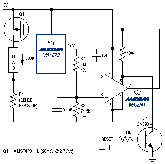 Figure 8. Low-voltage operation and speed (80ns propagation delay) make this comparator suitable as an overcurrent monitor in 3V systems. Some applications-monitoring a power supply's output voltage, for instance-require ultra-low power consumption rather than high speed. Maxim has designed a family of low-power comparators for this purpose. The MAX931-MAX934 comparator/reference ICs, for example, draw supply currents of only 3µA per comparator. Each device includes a voltage reference and one or more comparators with programmable hysteresis. The dual-comparator MAX932, for example, can implement an ultra-low-power microprocessor supervisory circuit (Figure 9). 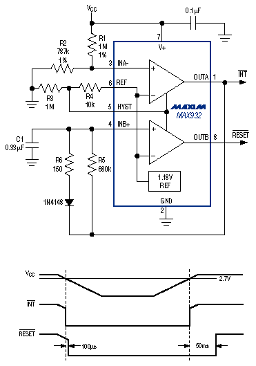 Figure 9. The MAX932-a reference and dual-comparator IC requiring only 6µA supply current-implements a micropower RESET generator. INT-bar goes low 100µs before the reset is issued. Other µP-supervisor ICs-even the lowest-power types that draw supply currents of 25µA to 100µA-may not be acceptable in applications that extend battery life by conserving every microamp of supply current. The MAX932 provides an accurate VCC monitor and power-on reset while drawing only 6µA. It also generates an interrupt (INT-bar) that precedes RESET-bar by 100µs. INT-bar gives the processor an early warning that allows the system to perform necessary housekeeping chores before resetting the hardware. For the early warning to work, VCC must not fall too sharply during the 100µs window between INT-bar and RESET-bar (as it may if the battery is removed abruptly). You should, therefore, bypass VCC with a capacitor to support the rail until the processor can execute a clean shutdown. The capacitor value depends on the load current. For 10mA loads, a 10µF capacitor allows VCC to drop only 0.1V during the 100µs interval. Microprocessor Supervisory Circuits Backup batteries, for example, ensure an uninterrupted flow of power to critical circuits (like the CMOS memory and real-time clock) when VCC is absent. By monitoring VCC, the µP supervisor decides when to switch the system over to the backup battery. Three-volt operation, however, presents an engineering problem that doesn't exist in 5V systems. Five-volt systems simply compare VCC with the backup voltage and switch to backup whenever VCC is lower. But, this approach can cause false switchovers in a 3.3V (or 3V) system: lithium backup batteries measure as high as 3.6V when fresh, which is higher than the 3.0V limit for VCC in a 3.3V system. Maxim supervisory circuits avoid this problem by allowing the backup voltage to exceed VCC, and initiating a switchover only when VCC falls below 2.4V. Circuits of this type are the MAX690R/S/T, MAX704R/S/T, MAX802R/S/T, and MAX804-806R/S/T. (R, S, and T suffixes denote different VCC monitor thresholds.) All come in 8-pin DIP and SO packages. On-board functions include backup-battery switchover, reset generation, watchdog timing, power-fail warning, and manual reset. Power-fail comparators for the MAX802R/S/T, MAX804R/S/T, and MAX806R/S/T ICs have ±2% accuracy, enabling them to monitor both the 3V and 5V VCC voltages in a dual-voltage system (Figure 10). In this circuit, the main VCC comparator monitors the 3V supply, and the power-fail (PFI) comparator monitors the 5V supply. 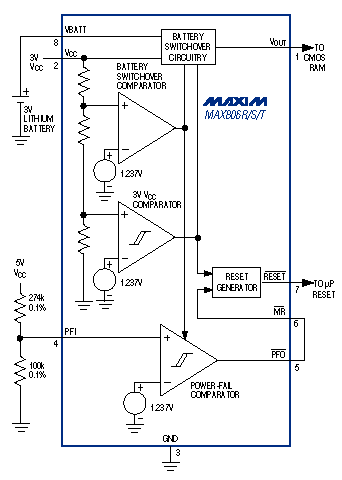 Figure 10. Configured as shown, this microprocessor supervisor monitors 5V and 3V VCC in a dual-voltage system. Internal circuitry issues a reset when the 3V VCC goes out of tolerance. The 5V VCC's trip threshold (4.527V to 4.726V) is set by 0.1% resistors; when 5V falls out of tolerance, the PFI-comparator output (PFO) pulls down the manual-reset input (MR). Thus, an out-of-tolerance condition for either VCC causes the chip to issue a reset. Other 3V supervisors from Maxim protect the memory ICs with chip-enable (CE) gating. CE gating enables the supervisor to protect the memory by blocking read and write operations during power faults. The MAX792 and MAX820, for example, feature CE gating with a propagation delay through the supervisor of only 10ns. (Short delays allow slower, cheaper memories because the CE delay takes less of the memory cycle time.) These devices also offer manual reset, power-on reset, power-fail warning, and watchdog timing. For extremely cost-sensitive applications, the MAX709 supervisor is available at $0.70 each for 25k pieces, direct from the factory. It comes in an 8-pin DIP or SO package. The MAX709 replaces the TL7705, including an external resistor and capacitor necessary for setting the TL7705's timeout period. Voltage
References The MAX872 can source or sink 500µA, with a corresponding guaranteed load regulation of 0.5mV/mA (source) and 12mV/mA (sink). Temperature drift is 40ppm/°C, and line regulation is 80µV/V over the 2.7V to 5.5V input range. For 5V operation, Maxim offers a wider selection of voltage references, along with the 3V-to-5V DC-DC converter that may be required. Three-terminal references generally allow lower operating currents than do the two-terminal types based on zener diodes. The three-terminal MAX872 draws 15µA, for instance, and the two-terminal LM385-2.5 draws 30µA. But, the operating currents can vary greatly according to the application-particularly if the input voltage varies, as it does for many battery-powered products (Figure 11). 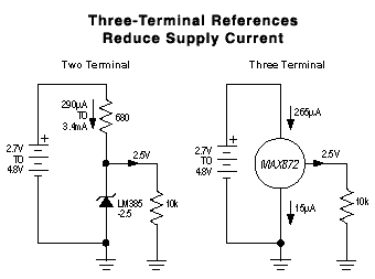 Figure 11. A 3-terminal voltage reference, unlike a 2-terminal type, draws constant supply current as the input voltage varies. When connected between a 10k Analog
Switches MAX391 parts are fabricated in a (relatively) low-voltage process whose thin gate oxides allow tight control of the gate threshold voltage (about 0.6V). The resulting internal MOSFETs are fully enhanced at 1.2V, and therefore function well at 3V (Figure 12). 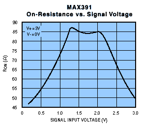 Figure 12. On-resistance for the MAX391 is superior to that of other low-voltage switches. DC/DC
Converters Linear regulators are simple, but they require an input voltage greater than the output. Charge-pump converters use capacitors for energy storage, and therefore provide small, low-cost, DC-DC conversion circuits. Die-size limitations, however, restrict the use of charge-pump converters to low-power applications. Switching regulators provide single or multiple outputs, controlled by PFM (pulse-frequency modulation), PWM (pulse-width modulation), or both, depending on the output power level. PFM (or pulse-skipping) control schemes, which allow high efficiency with light loads, allow the regulator to operate with quiescent supply currents as low as 10µA. PWM schemes consume more power, but they allow a fixed-frequency operation that yields high efficiency with heavier loads. Some converters provide excellent efficiency for both light and heavy loads by switching between the two control schemes according to the load-current level. For low-current applications, the simplest solution for boosting 3V to 5V is a capacitor-based regulating charge pump (Figure 13). The industry-standard 7660 and most other charge pumps don't regulate VOUT, but the MAX619 includes an analog reference and error amplifier whose output controls a set of internal switches connected to external capacitors. The switch/capacitor network can double or triple VIN, and the MAX619 regulates by switching between these modes of operation. As indicated, this circuit produces 20mA at 5V ±4%, for inputs that range between 2V and 3.6V. For inputs between 3.0V and 3.6V, the output-current capability is 50mA. 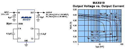 Figure 13. Occupying less than 0.1in.2 of area, the MAX619 regulated charge-pump converter generates 20mA at 5V ±4% for inputs of 2V to 3.6V. (From 3V to 3.6V, the output capability is 50mA.) Small size makes the Figure 13 circuit ideal for portable applications. The MAX619 comes in an 8-pin DIP or SO package, and the entire circuit (including the four external capacitors) occupies less than 0.1in.2 of board area. Operating current is 150µA, and shutdown current is only 1µA maximum. Input and load are disconnected during shutdown. To generate more supply current, you can opt for an auxiliary switching regulator such as the MAX761. Systems that handle bipolar signals usually require a negative supply, which can be generated locally if necessary. Again, the simplest solution is a charge pump such as the MAX660 or ICL7660. To provide more supply current, however, you need a switching regulator such as the MAX774. And if noise is a problem, you might consider shutting the regulator down at critical moments (Figure 14). 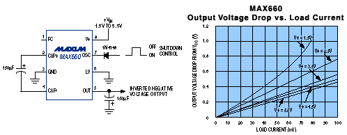 Figure 14. To eliminate noise in a downstream A/D converter, the MAX660 inverting charge-pump converter can be shut down between conversions (the output capacitor supplies current during that time). Shutdown control is available on many switching regulators. It comes in handy on the negative supply for an A/D converter, for instance. You can avoid the regulator's noise by simply shutting it down during conversions. The output capacitor supports the negative supply voltage during those intervals. Deriving 3V from higher input voltages requires either a linear regulator or a step-down (buck) switching regulator. Linear regulators are simpler, less noisy, and less expensive, but they dissipate more power (and generate more heat) as the applied input voltage rises. Linear regulators, however, can be quite efficient for applications with a low input-to-output differential (efficiency equals VOUT/VIN). A new family of linear regulators (MAX882/MAX883/ MAX884) incorporates several features of concern in the design of portable equipment: small size, low dropout, and low supply current. They supply 300mA of output current, and come in high-power SO packages that can dissipate up to 1W (vs. 450mW for conventional packages). Output voltages are 3.3V, 5.0V, and 3.3V, respectively. The p-channel-MOSFET pass transistors in MAX882/ MAX883/MAX884 devices help to achieve low supply current. Unlike the pnp-bipolar pass transistor found in conventional regulators, the MOSFET has no base-current overhead. MOSFETs also avoid the massive base-current losses contributed by pnp transistors when the regulator's input-to-output differential is low. Other features include a low-battery detector, an 8µA standby mode that turns off VOUT but keeps the low-battery detector active, and an off mode that turns off everything, lowering the supply current to less than 1µA. Linear regulators are efficient for low values of (VIN - VOUT), but for many applications the input voltage is considerably higher than the output voltage. Efficiency dictates a switching regulator in those cases, but switchers generate noise. RF applications such as radios and cellular phones, for example, must not include switching regulators that introduce noise at the sensitive IF frequency. An ideal choice for these RF applications is the MAX748A switching regulator. It delivers 500mA at 3V from inputs of 3.3V to 16V, with efficiencies that range from 85% to 92%. The output voltage is guaranteed to be free of subharmonic noise, and guaranteed limits on the internal oscillator frequency (159kHz to 212.5kHz) assure an absence of noise in the vicinity of 455kHz-an IF frequency found in radios and cellular telephones. An efficient buck regulator is also a good choice for upgrading an existing logic board to accommodate lower-voltage, lower-power ICs. Typically, these boards have 5V available but require a 3V supply for the new low-voltage logic. A linear regulator can easily convert 5V to 3V, but for higher load currents the power dissipation is prohibitive. At 10A, for instance, the linear regulator would dissipate 20W and require a heatsink. High-efficiency switchers such as the MAX767 (Figure 15) deliver 30mA to 10A with efficiencies exceeding 90%, thereby eliminating the need for heatsinks. 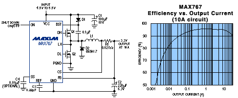 Figure 15. The MAX767 switching regulator converts 5V to 3.3V with efficiency greater than 90%. It supplies output currents to 10A, depending on the external components used. For external power control, the MAX767 employs low-cost n-channel switching MOSFETs instead of the lossier and more costly p-channel ones. Synchronous switch Q2 reduces loss in the Schottky diode (D2) by turning on when the diode conducts, but with a smaller forward-voltage drop. Because the diode drop would otherwise be a large percentage of 3.3V, Q2 greatly increases the regulator's efficiency. The MAX767 comes in a space-saving 20-pin SSOP package, and has an input range of 4.5V to 5.5V. Its quiescent operating current drops from 750µA to only 125µA in standby mode. High switching frequency (300kHz) allows the device to operate with small, low-cost surface-mount components. The 2.5µH inductor, for instance, is much smaller than that specified for competing ICs. Dual-output switching regulators are intended for systems designed from the beginning to operate with dual 5V and 3V supplies. Applications such as the generation of VCC voltages in a notebook computer, for example, are well served by the MAX782, which generates both of the regulated supply voltages (Figure 16). 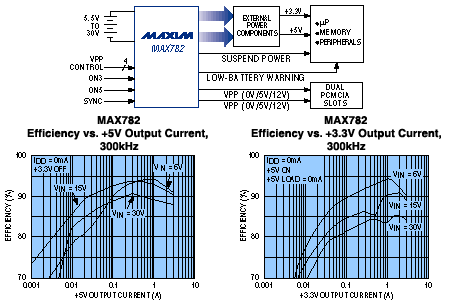 Figure 16. The MAX782 switching regulator generates dual 5V/3.3V outputs with efficiency greater than 90%. It also includes three precision comparators and a backup supply for RAM, and it generates dual VPP (PCMCIA) outputs. In addition to VCC, the MAX782 generates dual VPP (PCMCIA) outputs via a flyback winding on the 5V output. Other on-board functions include three precision comparators for low-battery detection, and dual, low-dropout linear regulators that supply backup voltages for the CMOS RAM and real-time clock. The greatest power consumption in notebook computers usually occurs in the 5V and 3V supplies, but this consumption varies over several decades according to the mode of operation: 5W to 15W during normal operation, and 25mW to 250mW during standby. The converter that generates these voltages, therefore, must maintain efficiency for a wide range of load currents. The MAX782 (Figure 16) does just that. The MAX782 achieves high efficiency with a combination of PFM (for light loads), PWM (for heavy loads), and synchronous rectification. PWM allows continuous current (an AC component superimposed on a DC offset) in the external inductor, which lowers the peak current and its associated I2R loss.1 At lighter loads, the converter reverts to the PFM mode and skips most of the oscillator pulses. By reducing the pulse frequency, it dramatically reduces the switching losses associated with the charge and discharge of gate capacitance in the external MOSFETs. The result is high efficiency at light loads. Many low-power applications require a VCC of 3V, obtained from a lower voltage or from a 3-cell stack (in that case, the input voltage ranges above and below VCC). MAX877 and MAX878 switching regulators excel in these applications (Figure 17). The MAX877/MAX878 incorporate an internal Active Rectifier™ that ensures regulation whether the input voltage is above or below VCC. The Active Rectifier™ also provides a complete disconnect between input and output when the regulator is shut down. (In most step-up DC-DC converters, the rectifying diode provides a direct connection between input and output when the input voltage is higher.) 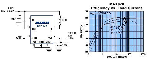 Figure 17. The MAX878 switching regulator's Active Rectifier™ enables it to deliver 250mA at 3.3V, from inputs that range above and below the output voltage. The MAX877 and MAX878 deliver 240mA at 3.3V, with input voltages from 1.5V to 6.2V. Efficiencies can be as high as 85%, and the 220µA quiescent supply current drops to a low 20µA during shutdown. These parts operate with small and inexpensive external components (an inductor and two capacitors) because the switching frequency is a high 300kHz. Other low-power applications require a switching regulator that starts (and operates) with a 1V input. MAX778/MAX779 devices meet this requirement; they start at 1V with a 10mA load, and require only three external components. Each part has an internal npn power switch. They can deliver as much as 300mA at 3V or 3.3V, and their low supply current (190µA) lets them achieve efficiencies as high as 80%. For low-voltage systems that must also generate PCMCIA or LCD voltages, you should choose from the MAX717-MAX723 family of dual switching converters. And to implement a stand-alone LCD controller, choose the MAX749 in an 8-pin DIP or SO package: it operates from 2V to 6V, draws only 60µA, and provides a digitally adjustable negative output. 1Vargha, Douglas.
"Extend battery life while minimizing size in portable equipment power
supplies," Part I, PCIM Magazine, March 1993, p.31. ™Active Rectifier is a trademark of Maxim Integrated Products. ™Lap Link is a trademark of Traveling Software.
| ||||||||||||||||||||||||||||||||||||||||||||||||||||||||||||||||||
|
|