Difference between revisions of "Spin Flip/Logic Electronics"
From Hall A Wiki
| Line 1: | Line 1: | ||
| + | <noinclude> | ||
| + | ''This article also serve as part of [[Online Spin Flip|spin flip manual]].'' | ||
| + | </noinclude> | ||
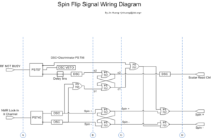
[[Image:Wiring Diagram.png|thumb|electronical design diagram]] | [[Image:Wiring Diagram.png|thumb|electronical design diagram]] | ||
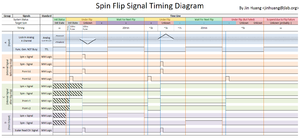
[[Image:TimingDiagram.png|thumb|timing of spin flip signal]] | [[Image:TimingDiagram.png|thumb|timing of spin flip signal]] | ||
Revision as of 17:52, 29 July 2008
This article also serve as part of spin flip manual.
The target logic electronics is designed as a standalone system, capable of extracting spin state information from target NMR signal induced during spin flip. The significance of this subsystem is that, in some unexpected case that the target computer should be down, these electronics could still keep a record of target spin information and ensure spin signal to DAQ is valid.
As shown in the electrical diagram and timing diagram,
- Input of this subsystem are
- RF function generator status signal (TTL Logic)
- Lock-In X channel of NMR (Analog)
- Output are
- 2 NIM logic signal, each stand for on spin state; if both of them is logical 0, then it implies the spin state is unknown
- One scalar read ctrl signal, which output a 100ns NIM logical 1 pulse during each successful spin flip. Now it's mainly used as counting number of flips.
- algorithm this electronics is based on, is the spin state of target have a fixed relation with sign of NMR signal.
- The key component is two Set-Reset Latches which lock down target state once a flip is confirmed

